Simplex-III

This is the all-TTL machine I built over 20 years ago. The entire thing fitted into some 120 TTL/MSI parts.
It was fully described in a series of articles in The Computer Journal (now defunct, alas).
This page provides a summary.
More home-built machines

Background

It all began in 1968, when I was at University in Bangor, N. Wales. The entire campus possessed just two machines (Elliott 803 and Elliott 4130), each of which filled a large room. Students punched their own programs (usually in Algol) on cards or 5-track paper tape, and submitted them to the operators. This whetted my appetite for computing.
When I left University, I lost access to a computer, and gradually developed the idea of building my own. There was a free-floating community of computer experimenters in the UK at that time. We made do with what could be found, and no two people's machines bore the least likeness to each other. Designs invariably were conditioned by what hardware we could lay our hands on. In those days, even basic 7400 logic parts were almost unobtainable by amateurs in the UK. DRAMs and EPROMs did not exist.

Simplex-I

I was fortunate enough to get hold of bits of some wrecked hardware from the early 1960's: logic boards from an old IBM mainframe, and most of a non-functioning VERDAN computer (that's a tale in itself: a military hybrid digital/analogue unit - used in SINS - Ships Inertial Navigation System). Both of these used discrete transistors, with one board roughly equivalent to an SSI package of today. There was also a disk memory unit for VERDAN: 2048 words of 24 bits each. Yes, this was a disk, with a separate head-pair for each track. The read-head was one sector's length before the write, so that a bit-serial CPU with a 1-word latency could do read-modify-writes to a single word on disk. That disk also implemented most of the VERDAN CPU registers, using a purely 1950's technique called "revolvers": a write head precedes a read head, so that the segment of track between implements a shift register. Several such registers may exist on a single disk track. The system clock was generated from a pre-recorded disk track, so that the entire system synchronised to the disk.

Design principles for my project derived largely from Booth's "Automatic Digital Calculators" - 1951 or thereabouts. Booth and his co-workers were building with vacuum tubes: the book is a mine of ideas on how to use as few gates as possible.

Having acquired a motor-generator to produce the power for the disk motor (115V, 400Hz 3-phase), I could start to run this thing up. A typical VERDAN PCB was a 8-bit shift register, so these were used unaltered. The architecture was pure 1950's: 7 serial "accumulators" (in the terminology of the time), and 2048 24-bit words of memory.

This project was later dubbed Simplex-I. It had reached the stage of having a working bit-serial arithmetic unit, when new vistas opened up.

Simplex-II

Having moved to London, I was able to obtain scrap hardware containing 7400 TTL chips. A London surplus dealer had a bin full of logic modules which he knew nothing about (and hence would sell for a song), but which I realised had been built at the place where I worked. So I had access to the manuals. Another surplus store provided a "no details" 4096 x 12-bit core memory array, and Simplex-II was under way. This was to be a virtual clone of a Digital Equipment Corporation PDP-8/S (for which I even had some software).

IO was a World War II surplus teletype machine (all of 7.5 chars/second).

Simplex-III

In late 1974, when Simplex-II was well along, I moved to Australia and the rules changed again. 7400 chips were now available at acceptable prices (via surplus dealers in the USA), and the first (1k bit) DRAM and EPROM chips were reaching the amateur market. Now I had spent my last 3 years in the UK working with the GEC 2050, at an engineering and assembly-code level, so I knew it thoroughly (including a collection of useful software techniques). Consequently Simplex-III was modelled on the 2050.

It was now 1976, and the Intel 8080 CPU was selling at $180. I thought long and hard, whether to use an 8080 anyway, but realised the cost would be little different, and a much better learning experience to do it myself. In those days, the only minicomputer (not micro) to use a stack was the PDP-11, of which I had no experience. So I stuck with the architecture I knew. The use of stacks as a subroutine linkage device was quite rare in those days also: most stacks were used as a data-handling device in compilers, and those were routinely emulated in software.

Naturally, there was considerable input from various friends during the design phase, not least in the form of a "wish list". Many saw themselves as potential users of the machine, once it was built. One of those friends was into astronomy, and indicated he would like to do a lot of maths on very large numbers. Largely for him, Simplex-III included arithmetic on integers up to 64 bits. There was never any intention to provide hardware floating-point maths.

The object was to provide much of the GEC 2050's functionality, with far less cost. I dumped the 2050's elaborate IO system (it had an in-built 64-channel DMA) and left everything memory mapped. The interrupt system again was vastly cut down, owing more to the Elliott 903 (another vintage machine, using discrete transistors).
In those days, no-one believed you could ever run out of 64kB main memory.

Simplex-III was based around TTL/MSI logic, and 1kb DRAMs. A design goal was to fit the microcode into two 32-byte bipolar PROMs. In the event, a PROM programmer was not available, so the PROMs were simulated by a discrete diode matrix, which connected to the PROM sockets.

The machine was built in a home-made case, approximately 380 x 200 x 200mm, including power supply and space for expansion cards.

Front Panel

Architecture

The GEC 2050 heritage suggested a register-to-memory architecture, in which every micro-cycle will run one DRAM cycle. This set the speed of the machine, and logically pointed me toward a very close memory/CPU coupling, where the main internal CPU clocks are so timed as to serve also as the RAS/CAS memory clocks. Those DRAMs were about 1uS cycle. The idea of using an 8-bit bus, with multi-precision arithmetic done by auto-indexing memory-address registers was borrowed from the 2050 (it was not novel to that, either). What I believe was my innovation was to do these multiple cycles not by loops in microcode, but by arranging that any microcode state (aka "box") could be repeated as needed. This vastly reduces the amount of microcode required. In the event, the entire microcode (including front-panel monitor functions) fitted in two bipolar 32 x 8 bit PROMs.
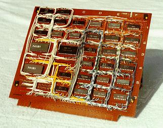
Typical logic board

Construction

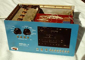
Simplex was hand-wired on 4 sheets of stripboard, approximately 150mm square. Each board had a standard load of 36 14/16 pin DIPs, with larger packages assigned more than one cell. The illustration shows the "Mill" card, which implemented the main data paths.
The boards were fitted in a backplane, parallel to the front panel. The front card carried the monitoring functions, with the display LEDs on a sub-board fitted to it.

Block Diagram

Organisation

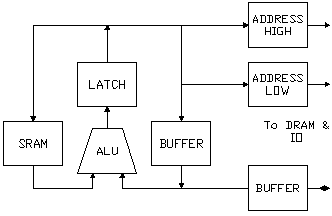
All the machine registers (except C) are in the SRAM at the left of the block diagram. "LATCH" is the "anti-race latch", needed as the SRAM was not edge-triggered: it did not do read-modify-writes.
The Address High & Address Low registers are chained as a 16-bit down-counter, enabling memory addresses to auto-decrement (recall, Simplex is big-endian) during multi-byte operations.

The DRAM refresh counter (not shown) multiplexed with the outputs of the low address counter.

Symbol Function Length
A Accumulator 1..8 bytes
X1 Address base 2 bytes
X2 Address base 2 bytes
X3 Address base 2 bytes
S Instruction counter 2 bytes
C Condition codes/flags 8 bits

Registers

All registers are duplicated for interrupt & base level working.

Memory can be addressed by a positive offset (0..255) from any of X1, X2, X3 or S.

Operation 4 bits
Index register 2 bits
Operand register 2 bits

Instruction Format

The 8 instruction bits are broken (in most instructions) into 3 fields as shown. The first operand is selected by the "operand register" bits, as A, X1, X2, or X3. The second operand is addressed in memory, by zero-padding the content of "LATCH" (the address offset), and adding the content of the "index register" S, X1, X2, or X3. As before, this addresses the highest (least-significant) addressed byte of the operand. As the operation proceeds, both the memory and SRAM address registers auto-decrement.
Relative jumps are executed in the same way, by taking an address forward or back relative to S, and storing that address in S.
For all registers except A, the data length is fixed at 2 bytes. A "length" register can be loaded, to define the length of A at anything from 1 to 8 bytes. Of course, this value simply defines the repeat count for operations involving A. The length value remains set until explicitly changed again.

Operation

A typical instruction proceeded by pulling the S register (in 2 bytes) from SRAM, incrementing it by 2 (all instructions were 2 bytes long), and posting the result back to SRAM, and to the two bytes of the Address Register. Two memory-read cycles followed, with the 16-bit address register auto-decrementing each time (Simplex is a big-endian machine, the MS byte is at the lowest address). This leaves the operation-code in the Instruction Register (not shown), and the address offset in the "L" register.

Instructions

Definitions:
z Content of object Z (register or memory)
Ro The operand register (A, X1, X2, X3)
Rx The index register (S, X1, X2, X3)
Q The effective memory operand address, defined as (rx + l)
q Content of Q

Where the target of an operation is shown as z, c this means the C (condition) bits are affected, as well as loading a result into z.
The instruction assignments are as follows:

CodeMnemonicFunctionNotes
0ADD ro + q => ro, c  
1ST ro => q  
2LD q => ro, c  
3XOR ro XOR q => ro, c 
4AND ro AND q => ro, c 
5LCP ro AND q => c ie as 8086 TEST instruction
6ADS ro + q => q, c  
7SUB ro - q => ro, c  
8CMP ro - q => c  
9JI/JILq => s See below for side effects
ACTS q + 1 => q, c Always 1-byte operand only
BSET   Set values for operand length, interrupt terminate, etc.
CRTL ro + ro => ro, c Add to itself, ie shift left
DBC s +/- l => s Direction, and condition set by Ro, Ri bits
ELDI l => ro, c  
FMIR ro + l => rx, c NB Effectively moves Ro to Rx
Side effects of the JI/JIL instruction. If Ro=X1, X2, or X3, store S in Ro (ie save subroutine link). Then or otherwise, q => s (indirect jump). If this instruction is executed in interrupt level, BOTH S registers are loaded.

Interrupts

Two copies of the SRAM (and C) registers exist, for interrupt and base-level tasks. At boot-up, the interrupt set are selected. Typically, the initialisation code ends with a JI instruction, which leaves both register-sets "S" regs. pointing at the same instruction. A SET instruction then drops to base level, which then over-writes the instruction at the JI target to jump to the interrupt routine. This interrupt routine is coded as a loop, which finishes with a SET [base level]. The following instruction will jump back to the head of the interrupt routine. Hence an interrupt switches register sets, and immediately jumps to the head of the interrupt routine. After the interrupt is done, the SET [base level] is executed, leaving the interrupt level's S pointing at its successor instruction, ie the jump back to head of interrupt.

Debug Support

Back in the '60s and '70s, the fancy debug software we have now was unknown, except perhaps on mainframes. We tested a program by stepping the hardware through the code. The same technique was used by service technicians to test the hardware. Accordingly, Simplex-III included a control/display panel, which could display any internal CPU register bit (using a type of Boundary-Scan access, using the DRAM refresh address as a scan counter, though BST was not invented then), and could halt execution on one of: The "boundary scan" mechanism ran continuously, utilising every bus cycle not consumed by the CPU proper. When the CPU is halted, the scan uses every bus cycle. The scan cycles are picked up by the RAM card, which uses them as refresh cycles (see below). Thus when the CPU halts, memory refresh and panel monitor operations are unaffected.

DRAM Refresh

This was built into the CPU, in that every microcycle which did not actually need the DRAM data bus, automatically ran a refresh cycle. Since all instructions included at least two such cycles (while the S was fetched and incremented), refresh was always guaranteed. Since the refresh logic operated independently of the microcode (it was in effect, interrupted to run a "real" DRAM cycle), refresh continued during CPU halts, even at the lowest microcode level.

Download Schematics

I have received several requests for a set of schematics to study. Please be aware that the original schematics were hand-drawn, and these files were digitised from the manuscripts. They are for illustration only, and are not electrically functional. All are in Adobe PDF format.

The original drawings have been scanned and added to this page.


Homebuilt CPUs WebRing

JavaScript by Qirien Dhaela

Join the ring?

To join the Homebuilt CPUs ring, drop me a line, mentioning your page's URL. I'll then add it to the list.
You will need to copy this code fragment into your page.
HomeBack to Home Page
Valid XHTML 1.0!