 Back to Home Page
DISCLAIMER |
|---|
| This information is provided strictly "as-is", and the author accepts no liability of any kind for events which may result from its use. No warranty of any kind is made regarding performance, freedom from faults, etc. |
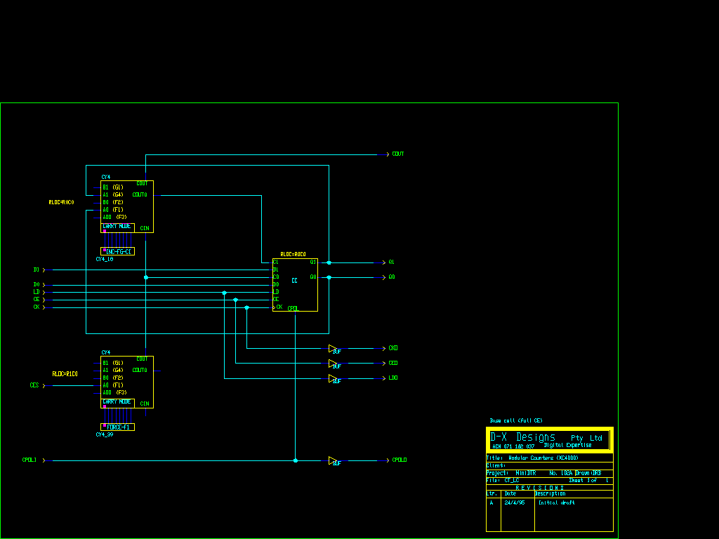
| CT_LC | 1st 2 bits of full-function counter |
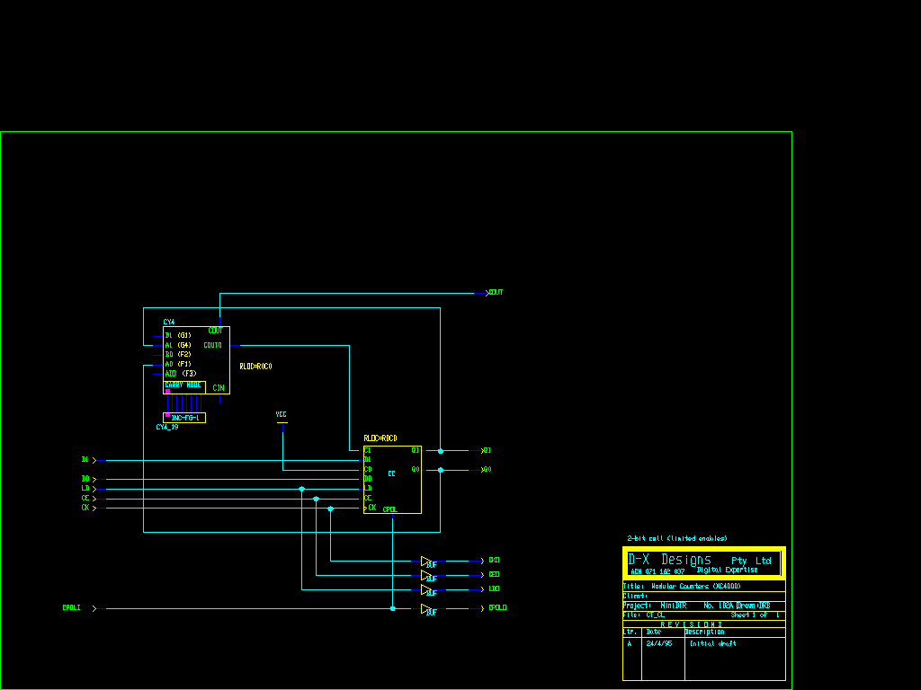
| CT_CL | 1st 2 bits of reduced-function counter |
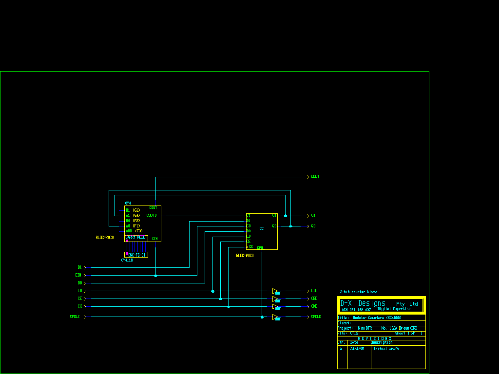
| CT_2 | 2 further counter bits |
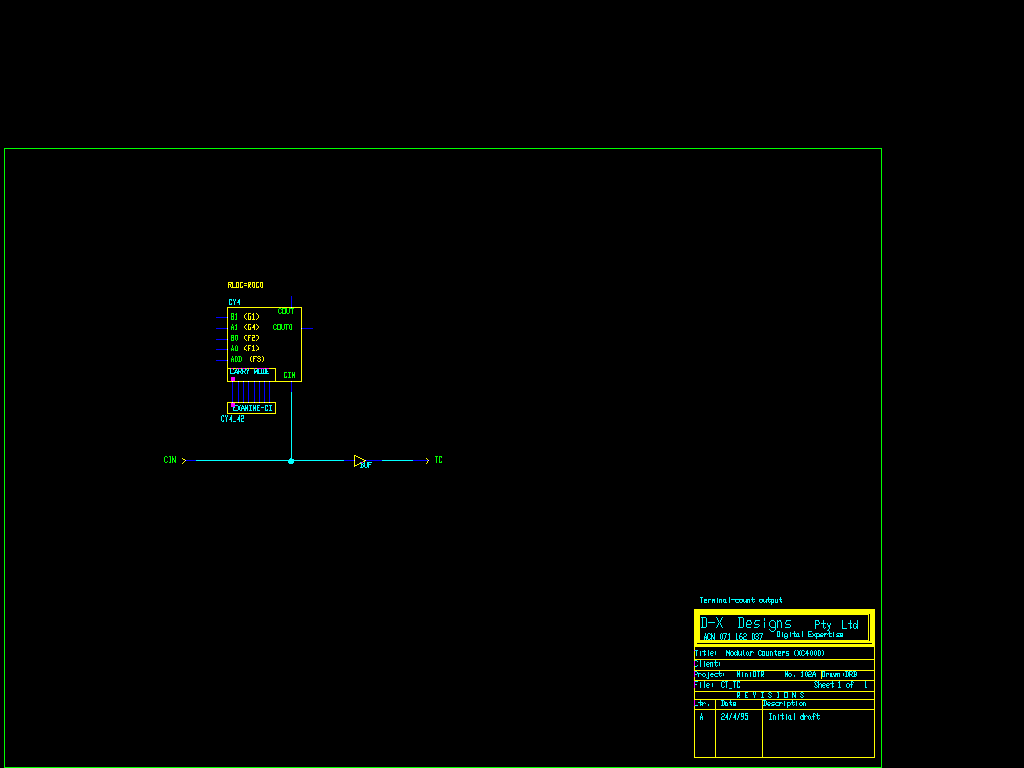
| CT_TC | carry-out (all ones) output (optional) |
| INPUTS | OUTPUTS | ||
|---|---|---|---|
| Signal | Significance | Signal | Significance |
| CPOLI | Clock polarity: HI for rising edge, LO for falling edge | Q0,1 | Parallel data out |
| CES | Secondary count enable | CPOLO | Clock polarity out (connect ONLY to next stage) |
| LD | Parallel load (dominates CES) | CO | Carry out (MUST connect only to following CIN) |
| CEP | Primary enable parallel (dominates everything) | ||
| CK | Clock | ||
| D0,1 | Parallel data in | ||
| OPERATION (when clocked) | |||
|---|---|---|---|
| CES | LD | CEP | Q0,1 |
| X | X | L | No change |
| X | H | H | D0,1 |
| L | L | H | No change |
| H | L | H | Increment |
| INPUTS | OUTPUTS | ||
|---|---|---|---|
| Signal | Significance | Signal | Significance |
| CPOLI | Clock polarity: HI for rising edge, LO for falling edge | Q0,1 | Parallel data out |
| CEP | Primary enable parallel (dominates everything) | CPOLO | Clock polarity out (connect ONLY to next stage) |
| LD | Parallel load | CO | Carry out (MUST connect only to following CIN) |
| CK | Clock | ||
| D0,1 | Parallel data in | ||
| OPERATION (when clocked) | |||
|---|---|---|---|
| LD | CEP | Q0,1 | |
| X | L | No change | |
| H | H | D0,1 | |
| L | H | Increment | |
| INPUTS | OUTPUTS | ||
|---|---|---|---|
| Signal | Significance | Signal | Significance |
| CPOLI | Clock polarity: HI for rising edge, LO for falling edge | Q0,1 | Parallel data out |
| CEP | Primary enable parallel (dominates everything) | CPOLO | Clock polarity out (connect ONLY to next stage) |
| LD | Parallel load | CO | Carry out (MUST connect only to following CIN) |
| CK | Clock | ||
| D0,1 | Parallel data in | ||
| CIN | Carry in (MUST connect only to preceding COUT) | ||
| OPERATION (when clocked) | |||
|---|---|---|---|
| LD | CEP | Q0,1 | |
| X | L | No change | |
| H | H | D0,1 | |
| L | H | Increment | |
| INPUTS | OUTPUTS | ||
|---|---|---|---|
| Signal | Significance | Signal | Significance |
| CIN | Carry in (MUST connect only to preceding COUT) | TC | Terminal carry (ie all counter bits =1) |
|
Back to Home Page
|
|
|