S100 Computers

HomeS-100 Boards HistoryNew BoardsSoftwareBoards For Sale
ForumOther Web SitesQuizIndex  
 
A Priority Interrupt Controller (PIC) and Real Time Clock (RTC) Board
Introduction

Most S-100 early systems did not use interrupts. Things like keyboard status were done by polling ports in software.  This works fine for simple systems where the CPU is typically occupied less than 20 % of the time anyway.  As systems got more complex with floppy and hard disk controllers, fast graphic boards and later multi-user systems the advantage of having a hardware interrupt driven system became quite apparent.   In these systems the CPU is interrupted on a priority basis by the hardware.  A well designed hardware driven interrupt S-100 system is quite impressive particularly in a multi tasking multi user 16 bit system like CPM86 or MS-DOS. Unfortunately creating a general interrupt system is not as easy as you may think both in terms of software and hardware.

Let's address the hardware first. Almost all CPUs have one or more pins to interrupt the CPU, and while there were/are a few specialized IC chips to collect and priories multiple hardware interrupts for the CPU. In practical terms the dominant Interrupt controller chip today is the Intel 5839A -- or its equivalent. The only other major candidate is the
AMD 9519. The latter is in fact a better and more flexible chip that works with almost any generic CPU. It was used in a number of early Z80 S-100 systems. However it never really caught on in the wider engineering community primarily because the original IBM PC used the 8259A and most software has since been centered around that chip.  I decide to used that chip in my system.

Programming the 8259.
The 8259A chip was originally made by Intel and consequently is geared to presenting interrupts to an 8080, 8085 or 8086 like CPU.  This presents both hardware and software problems when interfacing to the Zilog Z80 CPU and other non-Intel CPU's.

8259A pinout
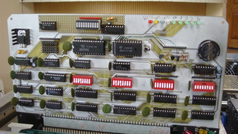
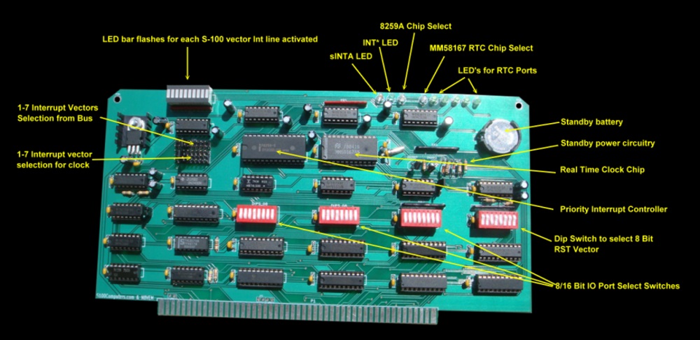
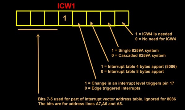
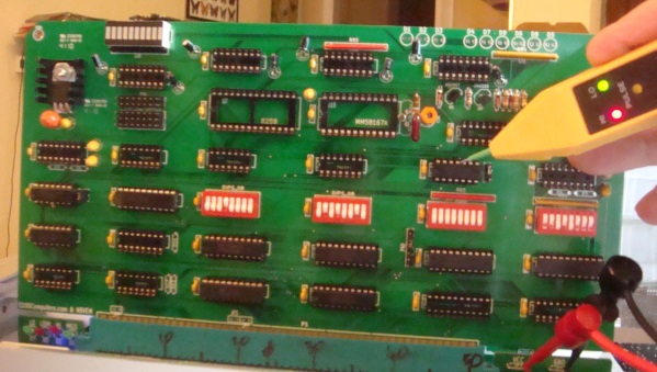
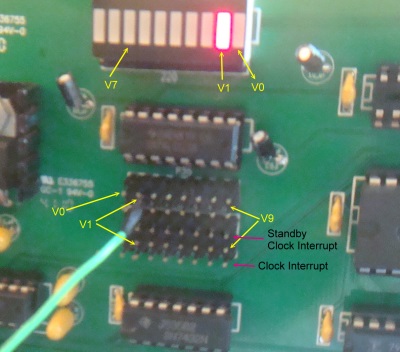
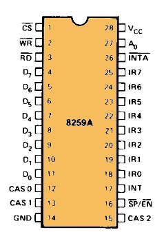
Lets first see how the 8259A works with an 8080 CPU. Please see the attached 8259A data sheet. The chip has 8 interrupt input pins. When any one of these is triggered  it MAY (depending on how the chip is programmed), pull the 8080 interrupt line low.  When this happens the 8080 will finish its current instruction and if interrupts are enabled in software acknowledge to the 8259 it got the interrupt request by sending a signal from its INTA pin which goes directly to the 8259.  Immediately after receiving this INTA signal the 8259 will put on the 8080 data bus a JUMP instruction (C3H).  The 8080 will then send two more INTA signals whereupon the 8259 will place low byte and high byte of data (programmed into the 8259) on to the data bus so that the 8080 sees these bytes as a JMP to a location XXXXH.   As far as the 8080 is concerned, the data bus appears to it as if it read memory asking for a JMP to a new location. At that location is software to handle the interrupt request. A return at the end of this software returns the CPU to where it was before the interrupt. The 8259 meanwhile is busy looking/processing any more interrupts.

So for an 8080 the 8259 expects and gets
three INTA signals to take over the data bus and redirect the CPU.   The Intel 16 bit 8086/80286 CPU's are different.  They send only two INTA signals when interrupted. Fortunately the 8259 can be programmed to understand this. The first INTA is ignored (in a single 8259A system, it is used by multi 8259A systems for a master/slave setup), but more importantly the CPU does not input any data from the bus after the first INTA.  After the second INTA an 8 byte "interrupt vector address" is place on the bus which the 8086/80286 CPU expects and uses to jump to a specific address in low RAM where it picks up a jump to the actual interrupt routine as described above.

The complication we immediately run into with the Z80 is that the Z80 only issues
one INTA after any interrupt.  In such a situation the 8259A would hang waiting for another two INTA's. Worse the Z80 would always get C3H on the bus (the first byte sent by the 8259A).  In order to address interfacing the 8259 to a Z80 we must first understand the strange (but powerful) ways a Z80 handles interrupts.

The Z80 actually has four different interrupt modes instead of the 8080's two (INT & NMI).  It has the NMI or non maskable interrupt mode exactly like the 8080 where if pin 17 is pulled low, the Z80 will always immediately jump to location 66H in RAM.  This mode is only used for power fail warning circuits etc and is not of much general use.  All other interrupt modes use the Z80 pin 16.

INT Mode 0.  This is identical to the 8080 Interrupt. If the Z80 is programmed to operate in this mode, it will expect a device to place on the bus after a single INTA signal -- one of the 8080's "RST vectors".  These are:-
 
 RST#OP Code Bit PatternRAM Location
 RTS 0C7 110001110000H
 RST 1CF 110011110008H
 RST 2D7 110101110010H
 RST 3DF 110111110018H
 RST 4E7 111001110020H
 RST 5EF 111011110028H
 RST 6F7 111101110030H
 RST 7FF 111111110038H

Very important, if no device places an RST 8 bit vector on the bus after the INTA signal, the bus will float (typically to 0FFH) and cause the Z80 to always jump to location 38H in RAM.

INT Mode 1.  This is a special Z80 interrupt which if the Z80 is so programmed to operate in this mode it will
always jump to location 38H in RAM.  This mode is very useful for testing software. Just temporally grounding pin 16 of the Z80 should force the CPU to jump to 38H in RAM.

INT Mode 2.  This is also a special Z80 interrupt which if the Z80 is so programmed to operate in this mode has an extremely powerful interrupt feature.  Again the Z80 sends out an INTA signal and expects to see an 8 bit vector on the data bus. However this time the 8 bit vector is combined with the special Z80 interrupt register "I" to generate a 16 bit interrupt vector address.  You should read up on the Z80 to learn more about this mode.  Suffice to say, it is far more elegant that the a 8080/8259A combination.  In this mode the Z80 can be forced to jump anywhere in its 64K address space.

So to recap. In Modes 0 and 2 the Z80 will expect just a SINGLE "interrupt vector" on the 8 bit data bus immediately after it issues an INTA signal.  On the S-100 bus, RAM memory boards must not respond to INTA as the Z80 reads the data bus.  


The Board
To test various aspects of the 8259A in the S-100 bus I first put together a prototype board (starting with our bear prototype board, see here).   Here is an early picture of that board.

PIC&RTC Prototype board

The board contains not only the 8259A interrupt controller but also a RTC (real time clock-calendar circuitry).  The RTC stuff will be described later.

The above special case requirement of the Z80 made it necessary for me to design two separate circuits for the PIC section of the board. One for a Z80 (one INTA issued) and one for Intel chips (two or three INTA's) issued.  I believe the Z8000 also issues two INTA's.  As I said above, early S-100 boards utilized the AMD 9519 PIC chip because it could be programmed to accept any number of INTA's.  However I wanted to keep the software compatibility of the 8259A for CPM86 and MS-DOS systems.

The solution was to utilize the 8259A in "poll mode" with the Z80 and hardware interrupt mode for 16 bit systems.  For Z80 interrupts an 8 position dip switch sets the default RTS vector (or mode 2) vector location the Z80 will jump to on the bus. At that location the Z80 will read the status port of the 8259A to determine which of the S-100's eight interrupts triggered the event.  See below for details.   In poll mode the 8259A keeps track of interrupts and prioritizes them etc. It also activates it INT pin which gets to the Z80 over the bus,  but it
DOES NOT expect any INTA signals returned back. A simple read of the status port acts as an INTA as far as the 8259A is concerned in poll mode.  The bits of the status byte read back have the following meaning:-

Bit 7,  6 ,  5,  4,  3,  2,    1,     0
     I    -    -    -    -  W2, W1, W0


where I=1 if the is an interrupt pending and W2-W0 is the binary code of the highest priority interrupt. Because we can use Mode 2 interrupts with the Z80,  you can essentially put your interrupt vector anywhere in the Z80 64K address space.

The core of the circuit is shown here:-

Z80 INTA Circuit

Upon receiving an interrupt on say the S-100 VI0 line, pin 18 of the 8259 will pulse high. This will cause the chip to issue an interrupt on its pin 17. The Z80 will receive this signal and return an sINTA signal.

Upon receiving the S-100 sINTA signal, U9 puts on the bus the appropriate bit pattern for RST 0 to 7 (
note, for Z80 Mode 0 interrupts, only bits 3-5 change) or, if we are using Mode 2 any bit pattern.  For example in Mode 0 if all switches of SW2 are set to ground except bit 5 the Z80 will jump to RAM location 10H on interrupt.  At that location (or a jump from that location) a "Poll command" is sent to the 8259A port (OCW3) . The next read from the 8259A port+1 returns the status register indicating which interrupt line was activated as described above. 

Now we don't want this process to occur when we are using another CPU (e.g.. a 8086). U12A tracks all the temporary master lines. Only when the Z80 master is controlling the bus can U9 be activated as described above.  It assumes that if another CPU has bus control one of the TMA0-4 lines will be low. 

I have written a short "demo" program called MYPIC.ASM to illustrate the use of this circuit.  It can be seen here and obtained here.  Note this is by no means a robust program. Sections are simply commented out to add flexibility. Modify to experiment.

Utilizing the board with Intel CPU's.
If a CPU like an 8086 is controlling the bus things are more straightforward. As explained above, the 8086 will expect (and will get) two INTA signals from the CPU. The relevant circuitry is shown below.
 
8086 INTA Circuit
 
The 8259A must be programmed carefully to accept and process hardware interrupts. The program example above illustrates this in Z80 code. But you need to carefully read the 8259A documentation to really take advantage of this chip. 

With an 8086 for example running the bus, an interrupt is received by the inverter to pulse a high on one of the 8259's interrupt lines (pins 18-25). Again an interrupt is sent form pin 17 to the CPU over the bus.  However this time the 8259 will put on the bus a jump vector (via U6) upon receiving the second INTA signal.  The activation of U6 is a little complicate in the whole board circuit because it is also used by the boards RTC (see below) however for this part of the circuit U6 is activated by sINTA (and only if a Z80 is not the bus controller).
 
Note U7 and U8 are also activated by "normal" IO reads and writes to the 8259A.  Also while the board can be configured to any one of the 8086's 64K I/O ports, normally the ports will be 20H & 21H to be compatible with the original IBM PC.

I have written a short "demo" program called MYPIC.A86 to illustrate the use of this circuit with an 8086 CPU on the S-100 bus.  It can be seen here and obtained here.


A Real Time Clock Board.
Because the above PIC circuitry did not take up a full S-100 board I decided to add a real time clock/calendar chip to the board as well.  Now unlike the 8259A PIC chip there were a number of popular early RTC chips used on S-100 boards.  Amongst the most common were the OKI 5832, the National MM58167A, a whole range of Dallas Semiconductor chips (e.g. 12C887) and more recently the Epson chips like the RTC-72421.

Which one to use? For me the decision was not hardware but software.   I have for years used the MM58167A on a SD Systems Serial I/O board with good reliability.  This board came with a Z80 code example of a driver for CPM+ file time and data stamping.  Because of the unusual way Digital Research processed and stored date information and the fact that a year 2000 correction was already done for this chip, I decided to stick with this chip and code, rather than rewrite the somewhat tricky code for another chip.  The only disadvantage of the 58167A is that it does not have leap year capability. Every 4 years you will have to correct the date in February.  That said, I have found the chip to be extremely accurate. It is seldom off more than a few seconds a month.

Programming the 58167A.
To the programmer the 58167A appears as a series of I/O ports (25 in all).  Each port (or "Register" as National calls them) contains information like seconds, hours, days etc.  Here is the complete list:-

58167 Registers 
 
The chip has 56 bits of non-volatile RAM to store information in power down mode. It also has two external interrupt pins to flag the bus CPU on specified occasions.  You should look over the data sheet in detail if you wish to work with this chip.  Back in the early 80's Steve Ciarcia described the chip in detail in Byte Magazine. It can also be seen in Volume IV of his Ciarcias Circuit Cellar book.

The Board
Adding the chip to the board from a hardware perspective was relatively straight forward.   The only complication being that one does not want to chew up almost a quarter of a Z80's available I/O port address space with 25 I/O ports. The way around this is to use only two ports. One port to select/point to the "current port" addressing the chip and a second port to actually access the data at that port on the chip.  To talk to the next chip port we increase the "pointer port" first.  This is done with a 74LS174 (U17) see the schematic here.  The relevant section can be seen here:-

58167 Circuit
 
Programming the chip is also straightforward. You can send data to any port in any order. For example to set the minutes. You first send to the 74LS174 port (in my case A0H), the value 03H to "point to" the minutes register.  You then send  the minutes data to port A1H to actually place the data in the 58167A register.  Sounds simple, it is except for one thing, the real time counters are divided into 4-bit digits with 2 digits being accessed during any read or write cycle. Each digit represents a BCD number and is defined precisely in the chips data sheet. Any unused bits are held at a logical zero during a read and ignored during a write. An unused bit is any bit not necessary to provide a full BCD number. For example tens of hours cannot legally exceed the number 2, thus only 2 bits are necessary to define the tens of hours. The other 2 bits in the tens of hours digit are ignored. 

To help understand programming this chip I have written a short Z80/CPM program that will:-

Display the current time.
Allow you to set the time and data
Display all the "raw" chip registers on the screen. 


This program called MYRTC.Z80 can be seen here and downloaded here.  Here is an example of the display output:-

RTC Diagnostic

Using the RTC chip for CPM file Time and Date Stamping
One of the really nice features of CPM+ (CPM3) and CPM86+ was that you had the ability to time and date stamp files on a hard disk. We take this for granted today with our current operating systems but early versions of CPM did not have this feature. 

The complication we have however is that CPM does not store the date information in a format that is compatible  with the registers in the 58167A (or any other RTC chip for that matter).  Instead it stores days in a screwball format consisting of a 16 bit binary number since January 1, 1978. To get the actual date you must convert this number to your own MM/DD/YY format.  Since CPM requires this binary number to be stored somewhere in hardware we store it in the 58167A onboard RAM. We use the chips RAM minutes store (register, 01011H) to store the CPM's low byte days count and the chips RAM hours store (register 01100) to store CPM's high byte count of days since January 1, 1978.  The days of the month (address 00110) register (and RAM store) and months register (address 00111) (and RAM store) are set to zero.

Say the system is not booted for days.  With the battery backup the chip will continue to function. If days go by, it will increment the days (and if necessary) months registers.   The next time CPM is booted up it will check these two locations. If they are not zero, the extra days will be added to the above 16 bit total days count, the new count will be stored in the chips RAM and the days of the month and months registers (and RAM stores) reset to zero.   This way CPM always has the correct date without the need for any operator input.

The complication is that the chip registers for the day of the month and month are invalid (usually 0).  In my MYRTC/CPM example I do not change these registers instead I display what CPM will see.  Here is an example:-

58167 Registers2
 
You can of course easily modify the program to use the chip as it was intended bypassing any CPM involvement and do without file time and date stamping (or store the information in non-volatile RAM somewhere else in your system, calculating days in software since the last system boot up).

Finally here is my CPM3 BIOS driver utilizing the clock. You can view it here and download it here.


A Production S-100 Board.
Realizing that a number of people might want to utilize a board like this (and the fact that I have 2 other S-100 systems that could use one) together with Andrew Lynch at N8VEM (see here) we made a draft of a "proper" commercial type S-100 board.  See below:-
 
Second Prototype

This board had a few minor bugs.  When these were fixed it was apparent that there was space for a few other things. After a few weeks of debugging and tweaking a second prototype board was made. Here is a picture of that board:-

Final Prototype PIC-RTC Board
The board is now finished. It appears to work rock solid in both 8 bit (Z80) and 16 bit systems (8086/80286).   Here is a general map of the boards layout:-

PIC-RTC Board Layout
Realizing that one of the difficulties working with interrupts is that sometimes things die and you don't know what is going on. With this board I have utilized a number of 74LS123 "single shots"  so the appropriate LED's flash whenever a signal appears on the bus/board no matter how short it is. This I found really makes writing software for the 8259A.

Programming the 8259A.
Unfortunately programming the 8259A is a little tricky. It does not have a typical hardware reset/clear pin and must be initialized carefully every time in software.  The chip is setup by sending a series of software commands ("Interrupt Control Words or ICW's" as Intel calls them) to the chip.  The order in which the ICW's are sent as well as which of the two ports of they are sent to is critical.  If you intend to program this chip please first read the Intel documentation which can be obtained here.

Here is a brief summary of the commands however to give you a flavor:-

Interrupt Control Word 1 (ICW1).
ICW3

This control word initialized the 8259A. Whenever it receives a command at it's port
A0 with a 1 in bit position 4 it immediately resets the chip. This command tells the chip what type of CPU it will be communicating with.

Interrupt Control Word 2 (ICW2).
ICW2
This command is always the second command and is sent to the chips
A1 port. It tells the chip where in memory the interrupt vector table is placed. Eight bit systems can have the table anywhere in its 64K space. The 8086 family can only have it in low RAM (0-400H).

Interrupt Control Word 3 (ICW3).
ICW3

This control word sent to address
A1, is really for more complex systems which have cascaded multiple 8259A's connected to each other. It need not concern us here (all bits set to 0's) since we have no slave PIC's.  BTW, for some reason I cannot quite understand this control word must actually be sent with my 8 bit Z80 system. If it's sent with the 8086/16 bit system the 8259A does not work.  See my code examples below.

Interrupt Control Word 4 (ICW4).
ICW4
This is the final control word that is sent to the 8259A to start it up. Again it is always sent to the 8259A's port
A1.  The two most important bits are:- Bit 0', to define how many INTA's the chip will expect from the CPU (see above), and bit 1 which defines how the chip is reactivated after an interrupt.   The other bits are really for multi 8259A systems.  And can be set to 0's for us.

Unfortunately we are still not out of the woods. To actually use the chip you must then send it "Operation Command Words, (OCW's).  There are three of which two are commonly used. 

Operation Command Word 1 (OCW1)
OCW1
This command which can be sent any time after the 8259A is initialized determines which of the 8 interrupt pins can actually trigger and interrupt. It is sent to the chips port
A1 address. If all pins are to accept interrupts then 0H should be sent as OCW1.

Operation Command Word 2 (OCW2)
OCW2
This is a fairly complex command. Bits 3 and 4 are
ALWAYS 0 and it is sent to the 8259A's port A0. Most of the bits have to do with rotating the priority of which interrupt the 8259A will accept should any come together.  Normally one sends an OCW2 of 0H if you want the chip to automatically accept the next interrupt when it has completed processing a previous one. Alternatively you can send a OCW2 of 20H if you want the software to reactivate the chips ability to process the next interrupt.

Operation Command Word 3 (OCW3)
OCW3
This is another complicate OCW. Bits 7,4 & 3 must be as shown.  It is sent to the 8259A port
A0.  Bits 6 & 5 are usually set to 0,0. They are used in complex operations where interrupt priorities are switched around. Bits 0 and 1 determine which status register you actually see when trying to determine which interrupt triggered the chip.  See the software examples. The important bit for us is bit 2. If it is set to 1, the 8259A switches to "poll mode" see above. When set to 0 it waits for the normal INTA signal.

The Status Ports.
The 8259A  has 3 status registers which can be read from its two ports. Clearly with 3 registers and two ports something has to be first setup.

The Interrupt Mask Register (IMR)
This one is easy. Any time you read the 8259A port
A1 you get this register. It simply returns the mask setup by OCW1 described above. So if you want to check your chip hardware after setting it up as described above, whatever is sent to port A1 should be read back from port A1.

Interrupt Request Register (IRR)
This register is read back from port
A0. However you must first select this register by first sending an OCW3 to port A0 as described above. The IRR contains the levels requesting an interrupt to be acknowledged. The highest request level is reset from the IRR when an interrupt acknowledge has been granted. It sort of shows the queue order if multiple interrupts are piling up. I have never really used it!

In-Service Register (ISR)
This register is also read back from port A0. However you must first select this register by first sending an OCW3 to port A0 as described above. The ISR shows the priority levels of interrupts currently being serviced. It us updated when an EOI command is issued. Again unless you want to play around with the order in which interrupts are processed on the fly I don't bother with this register. By adjusting the Mask register and possibly OCW2 you can handle most situations.

That's it for setting up the chip in software. Please carefully look over the simple programs I have included. they should help you get going without too much of a learning curve.


Here is a video of the board processing a Z80 interrupts. You can see the CS (blue) LED lights up for the 8259A, the INT signal (green) and the sINTA (red) flicker with each interrupt. Also the right LED bar lights up indicating which interrupt line was triggered.  The program (MYPIC.ASM) just prints the "." character on the CRT is a continuous loop. Any interrupt on S-100 line V0 - V7 causes a hardware interrupt to be triggered and a jump to the appropriate subroutine in RAM.


Here is the corresponding video using an 8086 S-100 bus master with 16 bit code and utilizing the full power of the 8259A.  Loading this program is a bit tricky. Because I did not want to load and run it under CPM86 initially (it uses its own interrupts), I assembled it with Digital Research's ASM86.COM assembler. This generates a .H86 file. I then use my H86TOHEX file converter to generate a .HEX file which I load under CPM3 with ZSID.  Resetting the system and bringing up my 8086 monitor I jump to 500H in RAM where this program resides -- above the 8086 Interrupt vectors.  Sorry all this will be much clearer when we get to 8086 systems in the future.


Here is a video showing the use of the MM58157A clock chip to generate a 1 second interrupt that is picked up by the 8259A. The status ports of both chips are displayed.  Remember the appropriate V0-V7 interrupt line is shown in the LOWER 3 bits of the 8259A status port. The 7th bit signals an interrupt is present.  For the clock chip the fact that bit 2 of the status port is 1 indicates a 1 second interrupt.  Please read both chips documentation for more information.  Also study my code examples in detail.  You can see the code here (and 8086 code here) and download it here. You really have to take care to set these chips up properly in software to get them working properly. Every bit counts!


A Production S-100 Board
Realizing that a number of people might want to utilize a board like this, together with Andrew Lynch at N8VEM (see here) we are now collecting names of people that might be interested in our next batch of boards. This will be the same as the board above except with Gold plated edge connectors i.e. a "proper" commercial type S-100 board.  If you want one please let Andrew or I know ASAP. They will be about $40 each. As always, you get your own parts, no hand holding or manual! 

Final Board and Board Assembly
Here is a picture of the final "Commercial Quality" PIC/RTC Board. 
 
Commercial Quality Board
 
Apart from the gold plated edge connector there were a few other minor tweaks.  One was a small 0-50pF trim cap to fine tune the clock crystal for more accurate timing.  This is a trial and error process. Turn it up or down a little each day if you find the seconds are off slightly. 

First solder in all IC sockets, resistors capacitors and jumpers.  Add the power regulator and 3V battery holder and battery. Check you are getting 5 volts to all IC sockets, At least 4.5 volts to pin 24 of U19 and when you computer is switched off at least 2.4 volts.

The board is in a sense two boards in one. So during assembly you may wish to get the PIC section done first. This uses ports 20H & 21H and the software MYPIC.ASM for testing.   Use MYRTC.A86 for testing  the 8259A with an 8086.

Later you can incorporate the RTC section using the ports A0H and A1H and the software MYRTC.Z80.

If you use the ports in the above software (20H,21H,A0H & A1H)  the switch settings should look like this:

Switch settings

Your board should look like this:-

Board before adding chips


Add the minimum chips to checkout port addressing. Add U10, U13, U20, U9, U16 and U18. Jumped P40 4-5 (and 2-3), K2 (1-2), and add jumper K1, (2-3) and JP4.  Most of the port addressing logic on the board is fairly straightforward.  For example in RAM at 0H put:-

D3, 20, C3, 00, 00  

and with a logic probe observe pin 11 of U30 pulse low if the switches and above jumpers are correct.
  
Testing Port 20H
    
In this arrangement P40 is jumpered 2-3 and 4-5 for 16 bit port addressing.  Jumper K2 sets the number of wait states put on the bus for I/O to the (slow) MM58167A chip.  I use 2 wait states with the 10MZ Z80 board (K2, 1-2).   If you use none,(no K2 jumper), you must bend up pin 4 of U10.

Jumper JP4 actually connects the INT output coming from the 8259A to the S-100 bus.   This of course is needed if you ever want to see an INTA coming back to pin 26 of the 8259A.
 
Once you have the port addressing working you can add U5,U22, U21, U23, U15, U12, U14, U8, U6 U24 and (U7 the 8259A0). Use the MYPIC.ASM software to check the 8 interrupt lines as I show in the video.

The dual row jumper of P36 serves no function normally. (There was actually an error in the board layout, one row was suppose to go to the S-100 bus and allow cross jumpering the INT vectors on the board to the eight 8259A inputs. Instead each pin on the top row is directly connected to the corresponding pin on the bottom row).  Anyway, in this version of the board they are connected (in pairs) directly to the S-100 bus's 8 Vector Interrupt lines. Grounding any one briefly will cause the corresponding S-100 Vector Interrupt to go low. This will lead to a flash on the LED bar and you should see that interrupt being recognized by the software (see below). 

The three rows below that, (P38, P37 & P39), are for connecting either, the RTC interrupt or RTC standby interrupt to any one of the S-100 vector interrupt lines.  Note P37 is between P38 and P39. See the schematic for details.  For example connecting any pin on the bottom row (P39) to the pin directly above it (P37) will cause the clock interrupt to trigger an S-100 interrupt on that line.
 
Interrup Pins
 
For the RTC section add all the remaining chips, particularly the MM58167.  Be careful with the pins of that chip they seem more delicate than most.  The MYRTC.Z80 software will allow you to configure the chip.

The board uses a coin type 3V battery to mention residual power for the MM58167A RTC. During normal operation of course the chip is driven from the 5V supply (via transistor Q1 and Diode D12).  It is important to put the transistors in the right way. Here is a close up picture:-

StandBy Power

The software supplied here is rudimentary for 8080/Z80 code.  Where this board will really shine is when we start using 16 bit CPU's with interrupt driven operation systems.  If you use this board and developed software for it please let me know so it can be used and appreciated by others.

All that remains to be done is add the indicator LEDs. I always just poke the LED's in their holes and check they are working before soldering them in. For INTS, LED's D1,2 & 3 should flash. The important LED is D1 the sINTA  signal coming back to the board letting you know the buses current master CPU recognized an interrupt and is in the process of determining what hardware INT vector to use.

LED's D4 to 7 are for the RTC port and chip address.   I have been using various versions of this board now for months. At least in my system it is very reliable.  I took the battery backup circuit from an SD Systems RTC board that had, granted, a much larger NiCad battery, but it still works 30 years since I bought it!
 
A Production S-100 Board.
Realizing that a number of people might want to utilize a board like this together with Andrew Lynch at N8VEM (see here) we have completed a run of these boards. We will collect names for a second batch if needed.  If you have an interest in such a bare board, let Andrew  know via e-mail at:-  lynchaj@yahoo.com
 
Please note all the above clearly applies only to people who know what they are doing and can  do a little soldering and board assembly.  There will be little hand holding at this stage.

Don Caprio has provided the following RCT-PIC Parts List.

The links below will contain the most recent schematic of this board.
Note, it may change over time and some IC part or pin numbers may not correlate exactly with the text in the article above.

MOST CURRENT PIC/RTC BOARD SCHEMATIC
(V11, FINAL, 9/23/2010)
MOST CURRENT PIC/RTC BOARD LAYOUT 
(V11, FINAL, 9/23/2010)

Other pages describing my S-100 hardware and software.
Please click here to continue...


This page was last modified on 06/03/2011